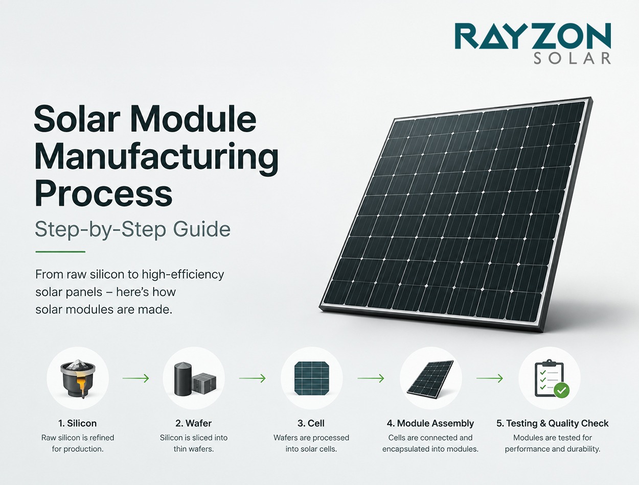
Solar Module Manufacturing Process: Step-by-Step Guide
The solar panel manufacturing process has emerged as a cornerstone of India's ambitious clean energy strategy. As the nation targets a monumental 500 gigawatts of non-fossil fuel electricity generation capacity by 2030, building a resilient domestic supply chain has transitioned from a policy preference to an absolute economic necessity. For project developers and commercial enterprises, evaluating the solar panel manufacturing process is essential to ensuring long-term asset reliability and maximizing capital efficiency.
As local production expands, the solar module manufacturing process must comply with strict state-enforced regulatory frameworks, such as the Approved List of Models and Manufacturers (ALMM) and Domestic Content Requirements (DCR). Choosing a reliable solar manufacturer is equally important as understanding the production process.
Explore premium solar solutions fromRayzon Solar.
A comprehensive grasp of the solar PV manufacturing process is vital for modern energy developers navigating the shifting landscape of international supply chains. To ensure top performance, analyzing the manufacturing process of solar pv module systems is key to mitigating risks associated with material degradation and physical microcracks.
This guide provides an exhaustive review of the solar panel manufacturing process in India, showcasing how raw silicon is transformed into high-efficiency power-generating assets. By understanding these engineering foundations, stakeholders can optimize their purchasing decisions and accelerate the transition toward a decentralized, sustainable energy future.
What Is the Solar Manufacturing Process?
In defining the solar panel manufacturing process, one must examine the systematic physical and chemical transformation of raw metallurgical elements into highly structured semiconductor devices.The solar module manufacturing process refers to the mechanical consolidation of these individual semiconductor cells into encapsulated, weather-resistant glass-and-aluminum frames.
Historically, the solar pv manufacturing process was treated as a fragmented assembly line; however, modern manufacturing plants operate as highly integrated, automated ecosystems. By breaking down the solar panel manufacturing process steps, one can observe the sequential transition from quartz reduction to chemical texturing, electrical contact sintering, and lamination. 9 To explain the solar manufacturing process step by step, we must synthesize how atomic-level modifications culminate in robust utility-scale panels.
Note: The solar panel manufacturing process involves converting purified silicon into wafers, transforming wafers into photovoltaic cells, and assembling them into durable solar panels capable of generating electricity from sunlight.
Raw Materials Used in Solar Panel Manufacturing
Silicon – The Core Material
Silicon remains the foundational material of the solar industry because its semi-conductive properties are ideal for creating an electric field under sunlight exposure. Silicon is used because it has four valence electrons in its outer atomic shell, allowing it to form a highly stable and ordered crystal lattice. When exposed to sunlight, incoming photons excite these electrons, allowing them to flow freely and generate an electrical current via the photovoltaic effect. In addition to being highly abundant and non-toxic, silicon offers exceptional chemical stability and an optimal bandgap for conversion efficiency.
An analysis of the monocrystalline solar panel manufacturing process highlights how single-crystal silicon wafers maximize electron mobility by removing grain boundaries.
- Monocrystalline Silicon: Pulling molten raw material using the Czochralski growth method creates a continuous, single-crystal atomic lattice. The complete absence of grain boundaries allows charge carriers to flow with minimal resistance, resulting in superior efficiencies between 20% and 22.5% and a sleek dark appearance.
- Polycrystalline Silicon: In contrast, polycrystalline silicon is cast in multi-crystalline blocks. Slow cooling introduces randomized, multiple crystal boundaries (grain boundaries) that trap charge carriers, reducing total conversion efficiencies to between 15% and 17% and leaving a speckled blue aesthetic.
Other Essential Materials
Beyond the active semiconductor layers, a commercial module requires robust materials to protect the cells and transfer electrical currents. The primary structural components include:
- Glass: High-transmittance, low-iron tempered glass shields the cell matrix from physical impact (such as hail or wind loads) while permitting maximum passage of sunlight.
- EVA sheets (Ethylene-Vinyl Acetate): These act as thermoplastic encapsulants. Positioned on both sides of the cell matrix, they cure under vacuum heat to seal out moisture, protect against damp heat, and prevent mechanical stress.
- Aluminum frame: Made of anodized, corrosion-resistant aluminum to provide overall structural rigidity, mechanical support against heavy snow/wind loads, and secure grounding points.
- Backsheet: A multi-layer polymer film that provides critical dielectric insulation, protecting the rear of the panel from UV degradation, high voltages, humidity, and physical wear.
- Junction box: A sealed, weatherproof enclosure (typically IP67 or IP68 rated) that houses bypass diodes to protect cells from reverse-current hotspots during shading, while serving as the primary electrical connection terminal.
- Copper ribbons: Tinned copper ribbons are soldered to interconnect individual solar cells in series and parallel, efficiently collecting and transmitting the generated electrical current to the junction box.
Step-by-Step Solar Manufacturing Process
Evaluating the complete solar panel manufacturing process requires analyzing how chemical refinement matches up with automated mechanical assembly. A detailed breakdown of the solar panel manufacturing process steps reveals the precision required to produce high-efficiency cells. This section outlines the solar manufacturing process step by step from chemical extraction to certified modules. Looking at the overall solar pv manufacturing process, each cell represents a carefully tuned semiconductor junction.
Step 1 – Silicon Purification
The initial step of the solar manufacturing process is the reduction of high-purity quartz sand (SiO₂) in carbon arc furnaces to create metallurgical-grade silicon (MGS). This MGS undergoes chemical processing with hydrochloric acid to synthesize trichlorosilane gas (SiHCl₃). Fractional distillation purifies the trichlorosilane, removing trace boron and phosphorus. The gas is then thermally decomposed in a Siemens reactor, depositing ultra-pure polysilicon.
Solar-grade silicon is ultra-pure silicon used for manufacturing photovoltaic cells. This raw material must reach a purity level of 99.999% to ensure that thermal and chemical recombination of carriers does not limit solar cell conversion efficiency.
Step 2 – Ingot Production
Inside modern facilities, the monocrystalline solar panel manufacturing process relies on the Czochralski growth method to form high-purity cylindrical ingots. Purified polysilicon is melted in a quartz crucible at approximately 1420⁰C inside an argon-shielded vacuum furnace. A single seed crystal of silicon is lowered into the melt and slowly pulled upward while rotating. 4 The molten silicon mimics the seed's crystal lattice as it cools, forming a single, continuous monocrystalline ingot. Polycrystalline ingots, conversely, are cast in square ceramic molds where the silicon cools slowly to form blocks of randomized multi-crystalline structures.
Step 3 – Wafer Manufacturing
Once the single-crystal ingots are cooled, they are squared along their length to optimize the layout of pseudo-square wafers. 4 The squared ingots are sliced into ultra-thin wafers measuring between 130µm and 180µm in thickness using high-speed diamond wire saws. Diamond wire cutting minimizes kerf loss, which is the material sawdust wasted during cutting. After slicing, the wafers undergo chemical wet cleaning to remove any microscopic metal residues and saw-damage layers.
Step 4 – Solar Cell Manufacturing
Wafers are transformed into active photovoltaic cells through several distinct steps:
- Surface Texturing: The wafers are chemically etched in a potassium hydroxide (KOH) solution with specialized additives. This forms random microscopic pyramids across the surface, trapping light and reducing reflection losses.
- Doping and Diffusion: Wafers are treated at temperatures of 800⁰C to1000 ⁰C with gaseous phosphorus oxychloride (POCl₃). This diffuses phosphorus atoms into the p-type wafer, creating the crucial n-type emitter layer and establishing the p-n junction.
- Edge Isolation: Any wrapped-around emitter material on the wafer edge is removed via laser edge deletion or chemical etching to prevent short circuits.
- Anti-Reflective Coating: Plasma-Enhanced Chemical Vapor Deposition (PECVD) is utilized to apply a thin layer of silicon nitride (SiNx), which minimizes light reflection and passivates the silicon surface.
- Metallization and Firing: Silver and aluminum pastes are screen-printed to form contacts, followed by high-temperature firing at 700⁰C to 900⁰C to solidify the contact interfaces.
Solar cells convert sunlight into electricity using the photovoltaic effect, where photons excite electrons inside silicon material.
Step 5 – Solar Module Assembly
To understand the manufacturing process of solar pv module layers, one must analyze the mechanical stringing and encapsulation phase. During the solar module manufacturing process, individual cells are soldered together using copper ribbons to create strings. These strings are laid out onto a stack consisting of tempered glass, an EVA layer, a second EVA layer, and a backsheet. The stack is passed through a vacuum laminator at 140⁰C to 150⁰C to seal the components. An aluminum frame is added, and the junction box is installed. Modern Indian solar manufacturers like Rayzon Solar use advanced automation and strict quality standards for efficient solar module production.
Step 6 – Testing and Quality Control
Every completed module undergoes final verification. This includes Electroluminescence (EL) testing to detect microcracks, Flash testing to measure electrical output,
Potential Induced Degradation (PID) testing, and thermal load testing
|
Test Type |
Technical Purpose |
Operational Standard |
|
EL Test |
Detect microcracks, cold solder joints, and localized silicon defects |
Infrared imaging under forward bias |
|
Flash Test |
Measure electrical output ( |
Calibrated pulse solar simulator |
|
PID Test |
Ensure long-term reliability and eliminate voltage leakage |
High voltage bias under heat and humidity |
|
Thermal Test |
Validate physical stability against thermal expansion |
Temperature ramping from |
 ,
,  ,
,  )
)

Types of Solar Panel Technologies Used in India
Monocrystalline Solar Panels
The monocrystalline solar panel manufacturing process produces cells with high structural integrity and efficiencies between 20% and 22.5%. Monocrystalline modules represent premium options with a low temperature coefficient, which helps maintain high output in the warm Indian climate.
Polycrystalline Solar Panels
Polycrystalline panels feature a distinct blue appearance with efficiencies of 15% to 17%. While they are cheaper to manufacture, their market share in India has declined, accounting for less than 2% of total shipments as developers prioritize high-power modules.
TOPCon Solar Panels
Tunnel Oxide Passivated Contact (TOPCon) modules represent the dominant technology in India, accounting for over 70% of module capacity by the end of 2025. It introduces an ultra-thin silicon oxide tunnel dielectric and a doped polysilicon layer on the rear of the cell. This structure provides excellent passivation and carrier selectivity, pushing module efficiencies to between 22% and 25.5%.
Bifacial Solar Panels
Bifacial modules capture light on both sides, replacing the standard backsheet with transparent glass or polymer. This technology boosts energy generation by 10% to 30% when installed over reflective surfaces. While crystalline silicon dominates, the flexible solar panels manufacturing process represents an alternative thin-film segment, utilizing copper indium gallium selenide (CIGS) on flexible substrates to create lightweight, bendable designs.
|
Technology Type |
Efficiency Range |
Relative Cost |
Manufacturing Complexity |
Key Application |
|
Monocrystalline |
|
Medium-High |
High (Czochralski pull) |
Rooftops & limited spaces |
|
Polycrystalline |
|
Low |
Low (Casting block) |
Budget domestic installations |
|
TOPCon |
|
Medium |
Very High (Oxide layer) |
Commercial & utility projects |
|
Bifacial |
|
High |
High (Dual-glass lamination) |
Ground-mounted utility arrays |


Solar Manufacturing Process Flow Chart
To summarize the solar manufacturing process step by step, the following flow chart maps the progression from chemical extraction to certified modules:
- Silicon Extraction: Quartz sand reduced to metallurgical-grade silicon.
- Silicon Purification: Siemens gas distillation yielding 99.999% solar-grade polysilicon.
- Ingot Formation: Czochralski single-crystal growth.
- Wafer Cutting: Diamond wire slicing.
- Solar Cell Production: KOH texturing, (POCl₃) doping, PECVD ARC deposition, and contact firing.
- Module Assembly: Automated cell stringing, layup, and vacuum encapsulation.
- Testing & Certification: EL imaging, solar simulator flash testing, and mechanical load certification.
- Packaging & Dispatch: Sort-class packaging and delivery.
The entire solar manufacturing process can be visualized as a highly structured, automated sequence designed to produce high-performance clean energy generators.
Solar Panel Manufacturing in India
Analyzing the solar panel manufacturing process in India reveals a massive, policy-driven expansion of domestic capacity. Under the ALMM mandate, solar PV module capacity in the country has reached 172,592 MW as of March 2026, marking a dramatic increase from under 10GW in 2018. Domestic cell manufacturing capacity has also grown to roughly 27 GW by December 2025. Gujarat remains the hub of this manufacturing boom, hosting about 45% of India’s overall solar cell and module production lines. The scaling of the solar panel manufacturing process in domestic factories is supported by the ₹ 24000 crore Production Linked Incentive (PLI) scheme, which funds the development of integrated giga-factories. As India expands domestic solar production capacity, companies such as Rayzon Solar are contributing to the country’s clean energy transformation. Rayzon Solar operates an 11.3 GW module production capacity across its Karanj and Sava plants in Gujarat and is adding a 3.5 GW cell line and in-house aluminum frame production to further increase its vertical integration.
Challenges in the Solar Manufacturing Process
The execution of the solar panel manufacturing process involves navigating various technical and economic obstacles to deliver high-performing modules. Key general challenges include:
- High Capital Investment: Establishing integrated manufacturing lines requires enormous capital expenditure, particularly for upstream stages like crystal pulling and wafer slicing, which rely heavily on specialized, high-cost machinery.
- Raw Material Dependency: Polysilicon and wafer production remain highly concentrated in specific regions, leaving global manufacturers dependent on key raw material imports.
- Supply Chain Challenges: Volatile freight rates, logistics gaps, and strict customs protocols can stall the delivery of essential components like silver paste and solar-grade glass.
- Technology Upgradation: The rapid transition from older technologies like PERC to n-type TOPCon and next-generation heterojunction (HJT) lines forces factories to constantly reinvest in capital-intensive upgrades to avoid obsolescence.
- Efficiency Losses: Minimizing recombination at the metal-silicon interface and mitigating shading losses from screen-printed metal grid lines require advanced process control.
- Quality Consistency: Eliminating localized silicon defects, microcracks, and Potential Induced Degradation (PID) across millions of cells requires highly automated, 100% inline inspection workflows.
Indian Market Perspective
From an Indian ecosystem perspective, the solar panel manufacturing process in india faces a unique set of market-driven dynamics:
- The "Super Assembler" Dilemma: Despite possessing over 172.5 GW of module capacity, India’s polysilicon capacity is extremely low (~2 GW), forcing manufacturers to import over 90% of their polysilicon and wafers.
- Upstream Cell Deficit: Domestic cell manufacturing capacity (~27 GW) satisfies less than one-sixth of the total module capacity, resulting in four-fifths of India's domestic modules relying on imported cells.
- High Equipment Importation: More than 85% of advanced manufacturing machines, including crystal-pulling furnaces and PECVD coating reactors, must be imported.
- Regulatory Demands: Policies like the ALMM List-I and List-II mandates, along with the upcoming ALMM List-III for wafers in 2028, place immense pressure on manufacturers to quickly build fully integrated, local supply chains.
- Capacity Consolidation: The domestic market is heavily consolidated, with the top 10 solar manufacturers controlling 99.5% of India’s overall cell production capacity
Sustainability in Solar Manufacturing
Integrating ESG and sustainable manufacturing principles has become a core objective for forward-thinking clean energy companies. Transitioning the solar panel manufacturing process toward green energy involves minimizing the carbon footprint of factory operations. Purifying silicon and pulling monocrystalline ingots require high thermal budgets, prompting leading manufacturers to implement carbon footprint reduction strategies, such as powering their plants with solar energy, co-generation grids, and sustainable packaging.
In addition, water-usage optimization through closed-loop recycling reduces the environmental impact of chemical etching and surface preparation. Green manufacturing practices are also adopted throughout the production line by deploying automated resource optimization systems. Furthermore, circular economy recycling initiatives are focusing on end-of-life panel recycling, using thermal and chemical treatments to reclaim silver, copper, glass, and raw silicon, preventing toxic electronic waste in landfills
Future of Solar Manufacturing in India
Future advancements in the monocrystalline solar panel manufacturing process will focus on tandem cells (such as perovskite-on-silicon stacks) to exceed the theoretical limits of single-junction silicon. Additionally, the flexible solar panels manufacturing process is gaining momentum as manufacturers seek to commercialize lightweight thin-film designs on curved roofs and vehicles. To reduce import dependencies, the government has proposed ALMM List-III for indigenously manufactured solar wafers, taking effect from June 1, 2028. This will mandate the use of domestic wafers in local cell production, driving complete vertical integration across the Indian market.
How to Choose a Reliable Solar Panel Manufacturer
Evaluating the manufacturing process of solar pv module assemblies helps developers select a reliable manufacturing partner. When choosing a supplier, consider this comprehensive checklist:
- ALMM approval: Ensure the manufacturer is listed on the Approved List of Models and Manufacturers (ALMM) by the MNRE, which is mandatory for grid-connected projects in India.
- Manufacturing capacity: Select a partner with large-scale annual manufacturing capacity (gigawatt-scale) to ensure bankability, timely delivery, and long-term project support.
- Certifications: Verify that the modules comply with Bureau of Indian Standards (BIS) and global benchmarks (such as IEC 61215 and IEC 61730).
- Technology used: Look for manufacturers utilizing advanced n-type TOPCon, bifacial, or high-efficiency monocrystalline technologies that minimize shading losses and degradation.
- Warranty support: Confirm the availability of robust power output and product warranties, typically extending up to 25 to 30 years.
- Quality testing standards: The facility must employ strict quality testing standards, including inline 100% Electroluminescence (EL) and flash testing before and after lamination.
- If you are looking for advanced and reliable solar panel solutions manufactured in India, explore the product portfolio at Rayzon Solar.
Frequently Asked Questions
How are solar panels manufactured?
The solar manufacturing process step by step involves purifying raw silicon, melting and growing it into solid ingots, slicing those ingots into ultra-thin wafers, chemically treating the wafers to form active p-n cell junctions, and assembling those cells between protective layers of tempered glass, EVA encapsulant, backsheet, and aluminum frames.
What is the raw material used in solar panels?
High-purity silicon serves as the primary semiconductor material. Supporting structural materials include tempered glass, EVA polymer encapsulant sheets, anodized aluminum framing, backsheets, copper ribbons, and silver metal paste.
What is the photovoltaic manufacturing process?
The solar pv manufacturing process represents the chemical and mechanical conversion of raw silicon wafers into light-absorbing cells and fully assembled modules. It encompasses texturing to trap light, diffusion doping to create electrical junctions, and screen-printing metal grids to collect current.
How long does solar panel manufacturing take?
The core solar panel manufacturing process steps at the assembly level are highly automated and take just a few minutes per completed module. However, the upstream thermal processes—including silicon gas purification and Czochralski crystal ingot growth—require several days of continuous, high-temperature operation
Which type of solar panel is best in India?
Monocrystalline and n-type TOPCon panels are considered the best technologies in India due to their high efficiency (22% to25.5%) and lower temperature coefficients, allowing them to produce more energy in hot climates.
What is the role of silicon in the solar manufacturing process?
Silicon acts as the primary semiconductor absorber, capturing solar photons to excite electrons and generate direct current electricity.
Are Indian solar panels good quality?
Yes, the solar panel manufacturing process in India adheres to strict international standards (IEC) and domestic BIS regulations, ensuring high-quality, reliable modules.
What certifications are required for solar panels in India?
Modules require BIS certification and must comply with IEC 61215 for performance and IEC 61730 for safety. Grid-connected installations must source modules from ALMM-listed manufacturers.
What is the difference between solar cell and solar module manufacturing?
In cell fabrication, silicon wafers are chemically treated, doped, and metallized. In the solar module manufacturing process, these completed cells are connected, laminated under EVA, framed, and equipped with a junction box.
What is ALMM in solar manufacturing?
The Approved List of Models and Manufacturers (ALMM) is a mandatory certification by the MNRE, ensuring that grid-connected projects source modules from certified domestic facilities.
Does the flexible solar panels manufacturing process allow for water resistance?
Yes, the flexible solar panels manufacturing process utilizes waterproof polymer surfaces like ETFE and achieves IP68 waterproof ratings to protect components from moisture.
Conclusion
By examining these solar panel manufacturing process steps, stakeholders can better appreciate the complex technology that drives modern renewable energy systems. India's domestic solar ecosystem has undergone a remarkable transformation, transitioning from a heavy reliance on imports to establishing a gigawatt-scale manufacturing hub powered by protective policies and active private investment.
Ultimately, the quality of the solar panel manufacturing process governs the financial viability of solar installations over their 25-to-30 year lifespans. For solar developers, choosing partners who leverage advanced technologies like n-type TOPCon and maintain high vertical integration is the key to building resilient energy systems. Project managers are urged to explore Indian-made solar solutions and partner with trusted local manufacturers to drive the global clean energy transition.